SMPS EMI Full-Spectrum Troubleshooting Guide
In the practical development of switch-mode power supplies (SMPS), electromagnetic interference (EMI) is often one of the most challenging aspects for hardware engineers. The failing emission peaks observed on the spectrum analyzer in the EMC test chamber are, in physical reality, the result of interactions between the complex and excitation sources inside the power supply and the parasitic parameters of the circuitry.
Ray’s engineering experience: Treat the frequency bands below as a diagnostic starting point, not a substitute for separating CM and DM noise in the actual test set-up. Topology, cable arrangement, and the applicable limit determine the final mitigation.
Before tuning capacitors or adding ferrite beads, apply a practical layout rule of thumb: keep EMI filter components away from the transformer, heatsink, and high- switching loop whenever the mechanical design permits. To keep traces clean during layout, many designers place common mode (CM) chokes or X/Y capacitors too close to the power switching stage. This allows the transformer’s leakage flux (via mutual inductance ) and the high-voltage switching node (via parasitic capacitance ) to couple noise directly onto the L and N lines. Once spatial near-field coupling occurs, high-frequency noise can bypass the intended filter path and contribute to test failures.
Based on the frequency distribution characteristics of common mode (CM) and differential mode (DM) noise generated by SMPS, we can segment the entire spectrum to address issues from their physical root causes.
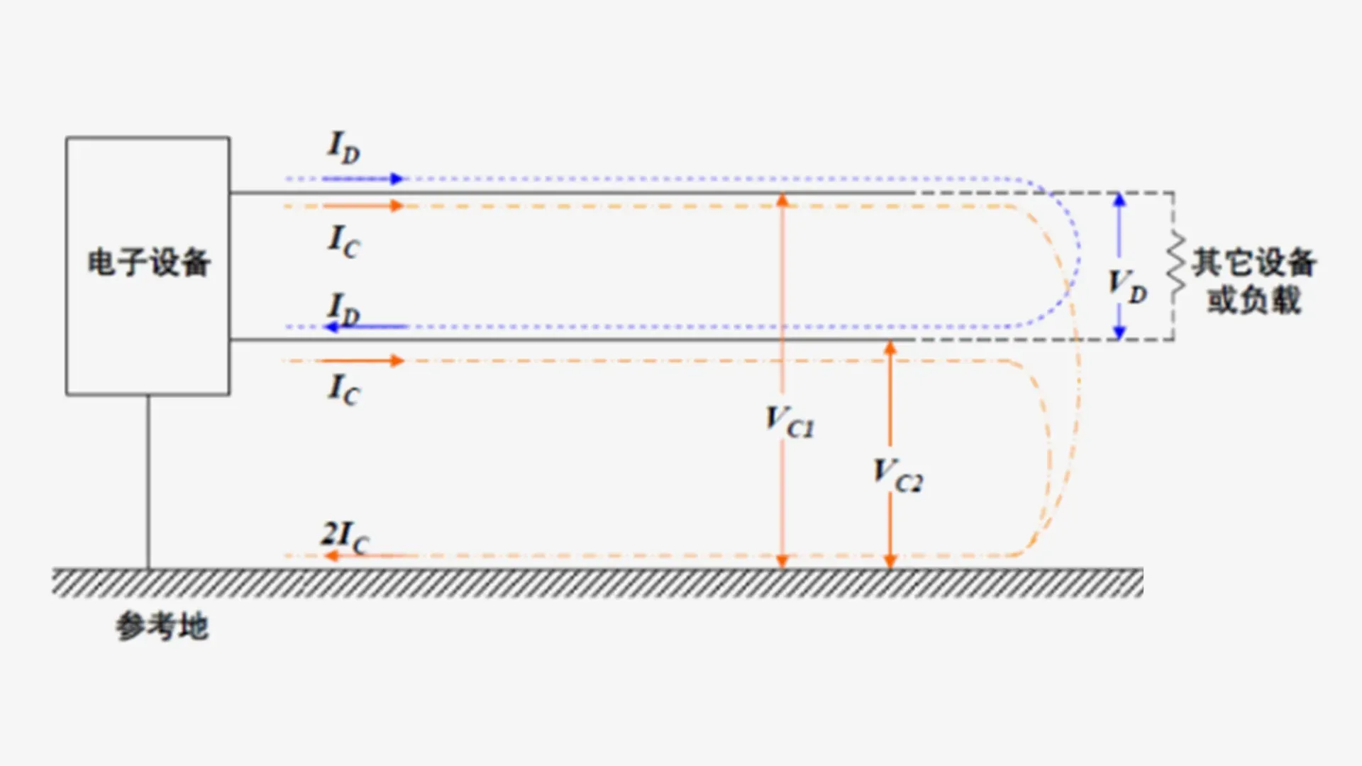
0.15MHz - 1MHz: Switching Frequency Harmonics & Differential Mode Dominant Region
In the low-frequency band below 1MHz, the dominant noise sources are the fundamental switching frequency and its lower-order harmonics. During this phase, the ripple current flowing between the line (L) and neutral (N) wires forms typical differential mode interference.
The Impedance Mismatch Principle & LC Low-Pass Filtering
The core physical logic for mitigating DM noise is impedance mismatch. The DM noise source (the input stage of the SMPS) typically exhibits low impedance. To maximize insertion loss, the filter must present high impedance on the side facing the noise source.
We can construct a low-pass filter by increasing the capacitance of X capacitors or by connecting differential mode inductors in series. For low-power supplies, a -type filter is commonly employed.
In practical engineering, it is recommended that the bulk electrolytic capacitor close to the primary-side rectifier bridge or the transformer have a larger capacitance and lower Equivalent Series Resistance (ESR), which can directly bypass a significant amount of low-frequency DM ripple current at the source.
1MHz - 5MHz: Mixed DM and CM Noise Transition Region
As the frequency rises into the 1MHz - 5MHz range, pure differential mode noise starts to decay, while common mode noise begins to rise because parasitic capacitances between the traces and ground begin to take effect. This is a transition zone where DM and CM noises coexist and intertwine.
Using a series of X capacitors (0.47μF or larger) in parallel at the input to filter out DM interference, we can analyze and resolve which type of interference is failing:
- If DM interference exceeds limits, tweak the X capacitance or insert a DM choke to optimize the filter’s corner frequency.
- If CM interference exceeds limits, add common mode chokes and select an appropriate inductance to suppress it.
5MHz - 30MHz: Capacitive Coupling Region of High-Frequency Common Mode Noise
Above 5MHz, DM components are virtually attenuated to negligible levels, and conducted EMI testing enters a region dominated purely by common mode noise. The main culprit in this frequency band is the high-speed voltage transition (high ) at the drain of the switching transistor (MOSFET).
Transformer Parasitic Capacitance & High-Frequency Return Path Impedance
As the MOSFET switches on and off in extremely short intervals, a voltage step of hundreds of volts is generated at the drain. This high-frequency voltage fluctuation couples to the secondary side through the inter-winding parasitic capacitance () of the transformer, subsequently flowing to the earth and forming a common mode current.
To suppress this high-frequency CM current, we have two engineering strategies:
-
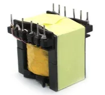
Break/Shield the Coupling Path: Introduce a copper foil shielding layer (Faraday Shield) inside the transformer, either at the innermost layer or between the primary and secondary windings. Note that the copper foil must form a closed loop (but must not short-circuit to create a shorted turn; insulation overlap is required), and it must be connected to the primary-side reference ground (Primary GND) via a short wire. This effectively intercepts , bypassing the displacement current that would otherwise flow to the secondary ground directly back to the primary side, dissipating it within an extremely small local loop.
-
Provide a Low-Impedance Return Path: Optimize the capacitance and physical placement of the Y-capacitor (Y1 or Y2). The Y-capacitor provides a low-impedance AC “shortcut” for the CM current that has already reached the secondary side to return cleanly to the primary side, rather than flowing back to the LISN via the L and N lines and causing test failures.
30MHz - 80MHz: Parasitic Loop Antenna Region of Radiated Emission (RE)
Above 30MHz, the wavelength becomes shorter. Although conducted testing concludes, the challenges of Radiated Emission (RE) testing begin. Test failures in this frequency band are physically caused by high-frequency current loops on the PCB acting as highly efficient loop antennas.
Damping in the Primary Power Loop
The “primary power loop”—consisting of the primary switch (MOSFET), the transformer’s primary winding, and the bulk electrolytic capacitor—is the primary radiator. According to the loop antenna radiation formula, the radiated field strength is proportional to the loop area. Therefore, the absolute layout rule is to minimize the physical area of the primary power loop.
If the loop area is constrained by physical space, we must suppress parasitic oscillations at the source:
- Increase the MOSFET Gate Drive Resistor (): By slowing down the gate charge and discharge rates, we intentionally reduce the and during turn-on and turn-off transitions. This is the most direct method.
- RC Snubbers & Ferrite Beads for Energy Dissipation: Parallel a 10-100pF high-voltage ceramic capacitor (or an RC snubber circuit) across the MOSFET’s D and S terminals to absorb voltage spikes generated by parasitic inductances. For higher power supplies, a chip ferrite bead can be connected in series with the MOSFET’s drain lead. Ferrite beads exhibit resistive characteristics (R-region) at frequencies above 30MHz, converting high-frequency oscillation energy into thermal dissipation.
Secondary Commutation Loop & Equivalent Antennas
The radiation source can also shift to the secondary side—specifically the “secondary power loop” consisting of the transformer’s secondary winding, the output rectifier diode, and the output electrolytic capacitor.
The mitigation strategies here similarly follow the principles of “minimizing loop area” and “reducing slew rates”:
- Minimize Secondary Loop: Strictly control the trace lengths from the secondary diode to the filtering capacitor.
- High-Frequency Absorption & Isolation: Parallel an RC snubber across the output diode to precisely suppress very high frequency (VHF) resonance between the diode’s reverse recovery and the transformer’s leakage inductance. A SMD ferrite bead can also be connected in series with the anode of the diode.
- Secondary Common Mode Interception: For adapters with a high-current single-rail output (whose output cables can easily act as long dipole antennas), it is highly recommended to add a common-mode choke (preferably wound with >3 turns of parallel wires) after the output electrolytic capacitor. This thoroughly chokes the VHF CM currents attempting to radiate along the output cable.
Above 200MHz
As for frequencies above 200MHz, since the energy of the SMPS itself is mainly concentrated in the lower frequency switching harmonics, the energy has already undergone multiple stages of natural low-pass attenuation due to parasitic parameters by the time it reaches this range. As long as the loop layout is properly controlled in the early stages, radiated emissions rarely exceed limits in this frequency band.
Doing EMC or RF Testing?
Use our free online engineering calculators to instantly convert dBuV, dBm, VSWR, Antenna Factors, and more.