A Must-Read Guide to System-Level EMC Pitfalls for Modern Hardware Engineers
A Must-Read Guide to System-Level EMC Pitfalls for Modern Hardware Engineers
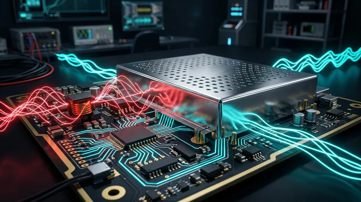
During the early stages of hardware R&D, we are often driven by product functionality and project schedule milestones. Many intuitions accumulated by engineers during the era of low-speed, low-frequency designs often fail in modern high-speed, high-frequency electronic design—a microcontroller and its peripherals, seemingly correctly connected in the schematic, crash repeatedly upon power-up; a prototype sent with full confidence to an EMC (Electromagnetic Compatibility) lab fails miserably in Radiated Emission (RE) and Electrostatic Discharge (ESD) testing.
Why does this happen? Because with the evolution of integrated circuit processes, even if the system clock frequency isn’t high, the rise and fall times of the chip driver pins have become extremely steep. Relying purely on logical circuit design thinking is destined to fail when dealing with the physical characteristics of modern hardware.
To ensure that a product not only “runs” on the first try but also “runs stably” in harsh electromagnetic environments, we must abandon the Band-Aid approach of “designing for functionality first, and relying on copper tape and ferrite beads in the lab later.” Real EMC design is a systematic engineering discipline encompassing everything from silicon die, PCB routing, ground networks, to chassis structures. Below, starting from the physical essence, we will dissect the five levels of electromagnetic compatibility design and engineering implementation laws from shallow to deep.
Level 1: Source Control (Active Component Selection and PCB Layout)
All electromagnetic interference (EMI) issues, in essence, are the unintended radiation and conduction of energy. To stifle the source, we must first look through the transient currents inside the chip and the frequency-domain characteristics of high-speed signals.
The Relationship Between Signal Edge Rate and Effective Bandwidth
In practical engineering, many engineers fall into a common intuitive pitfall: assuming that a 10MHz clock frequency is low and does not require high-speed routing. However, in the world of electromagnetics, what determines the high-frequency radiation energy is not the fundamental frequency, but the rise time of the signal.
We can derive a critical physical evaluation formula through the Fourier transform:
In this formula, represents the effective electromagnetic bandwidth of the signal (the highest frequency component of interest), and represents the rise time required for the signal waveform to rise from 10% to 90%.
This means that even for a 1MHz clock signal, if its rise time is only 1ns, its high-frequency radiation bandwidth will be as high as 318MHz or more. Interconnects must be able to transmit these high-frequency harmonics without distortion; otherwise, not only will signal integrity (SI) issues occur, but high-order harmonics will also radiate electromagnetic waves into space.
Synchronous Switching Noise (SSN) and Package Parasitic Inductance
When digital chip logic gates transition rapidly between “0” and “1”, they draw instantaneous currents from the power distribution network, known as noise. As this transient load current flows through the chip package and PCB traces, it triggers severe fluctuations in the ground and power voltages (Ground/Power Bounce). The underlying physical mechanism is Faraday’s law of electromagnetic induction:
In this formula, represents the spike voltage generated by the parasitic inductance of the trace (i.e., synchronous switching noise), represents the equivalent parasitic inductance of the power or ground loop, and represents the rate of change of current over time.
To mitigate this noise, simply adding decoupling capacitors is insufficient; we must reduce the system parasitic inductance . This requires us to pay close attention to IC package technology during component selection. From traditional DIP (Dual In-line Package, with extremely long pins and large inductance) to SMT, BGA, CSP (Chip Scale Package), and even SoC system-level bare die packaging, one of the core physical purposes is to compress the parasitic inductance between the chip die and the PCB pads to the absolute limit.
High-Frequency Return Paths and Loop Area Minimization
Current never goes out without returning; it must flow in a closed loop. At DC or low frequencies, current follows the path of least resistance; however, at high frequencies, current exhibits its physical instinct—following the path of least impedance (specifically, least inductance), which is typically the reference plane directly beneath the signal line.
The loop parasitic inductance is approximately proportional to the enclosed area:
Where is the loop inductance, is the magnetic permeability of space, is the loop area formed by the signal and its return path, and is the trace width.
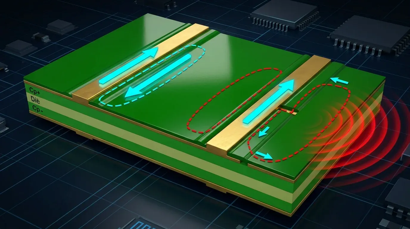
Therefore, we recommend following these strict rules during PCB layout:
- Minimized Loop Area: High-speed signals must have an adjacent, continuous GND or VCC complete reference plane (e.g., 4-layer boards or higher stackups), allowing high-frequency image return currents to tightly hug the signal trace, neutralizing differential mode radiation to a minimum.
- Avoid Routing Over Split Planes: It is strictly forbidden for high-speed signals to cross split areas in the reference plane. Once they cross a split, the return current is forced to detour, causing the to surge, multiplying the inductance, and turning the trace directly into a highly efficient “slot antenna.”
- Signal Integrity Constraints: Avoid abrupt trace width changes and right-angle routing to maintain characteristic impedance continuity. Use series or parallel termination resistors at the driver or receiver end to eliminate overshoot and ringing caused by signal reflections.
Level 2: Signal Network Architecture and Reference Ground Planes
In the high-frequency physical world, electromagnetic fields do not distinguish between “power,” “signal,” or “ground.” Any metallic conductor carrying high-frequency alternating currents (especially common mode currents) will completely lose its function as a transmission line or return path and mutate into a highly efficient resonant antenna radiating electromagnetic waves into space once its continuous physical length approaches a quarter-wavelength () of the signal.
Based on this physical essence, we must follow these frequency-domain boundaries and isolation guidelines in system topology design:
1. Low-Frequency Single-Point Grounding (Frequency < 1MHz): Preventing “Common Impedance” Crosstalk
- Physical Essence: In this frequency range (wavelength > 300 meters), transmission line effects are negligible. Conductor impedance is dominated almost entirely by DC resistance (R).
- Engineering Application: Applicable to low-frequency sensors, audio, and high-power motor drive circuits. To prevent large currents from generating voltage drops () on the common ground loop and “contaminating” the reference potential of weak signals, strict single-point or star grounding must be adopted to physically cut off the “crosstalk” path of low-frequency currents.
2. High-Frequency Multi-Point Grounding (Frequency > 10MHz): Disrupting “Antenna Resonance” Conditions
- Physical Essence: As frequency rises, parasitic inductance (L) and distributed capacitance (C) dominate. High impedance on a single wire leads to severe potential fluctuations (ground bounce), which in turn becomes the excitation source driving external conductors.
- Engineering Law: The uncontrolled continuous length of any internal trace or local shield carrying high-frequency noise must be strictly compressed to within .
- Implementation Strategy: High-frequency circuits must be “anchored” to the large, continuous reference plane (GND Plane) or metal chassis below using the shortest path through dense stitching vias or via fences. This is not only to lower return impedance, but also to force a change in the conductor’s electromagnetic boundaries and disrupt the antenna effect before its length reaches the dangerous resonance point.
3. Interface Common-Mode Filtering: Securing the Boundary (Cutting Off the “External Antenna” Feed Source)
- Core Pain Point: The physical size of internal PCBAs is often insufficient to act as an efficient antenna in lower frequency bands (e.g., 30MHz to 50MHz in CISPR 25). The real lethal antennas are the long external wiring harnesses connected to the PCBA (such as 1.7m power lines or communication lines).
- Implementation Strategy: Do not allow the fluctuating internal reference ground potential (common mode voltage) to directly drive the external wiring harness. At the connector interfaces between the PCBA and external long wire harnesses, we must establish a “customs barrier”:
- Blocking: Connect common mode chokes or high-frequency ferrite beads in series to choke high-frequency common mode currents.
Level 3: Structural Shielding Design (Spatial Electromagnetic Barrier)
When the source optimization on the PCB has been pushed to its limit and some high-frequency energy still leaks out, the chassis shield acts as a physical barrier to cut off radiative coupling paths. The essence of shielding effectiveness (SE) lies in the “reflection loss” of electromagnetic waves at the metal interface and the “absorption loss” inside the metal.
Skin Effect and Materials Absorption Loss Mechanism
As electromagnetic waves penetrate metal, their energy decays exponentially, governed by the physical law of skin depth:
Where is the skin depth (the depth at which the amplitude of the electromagnetic wave decays to of its surface value), is the angular frequency, is the material’s magnetic permeability, and is the material’s electrical conductivity.
This yields a clear guide for material selection:
- High-Frequency Electric Field / Plane Wave Shielding: Use materials with high electrical conductivity (large ), such as copper or aluminum.
- Low-Frequency Magnetic Field Shielding (e.g., < 100kHz): Since is very small at low frequencies, we must rely on materials with extremely high magnetic permeability (), such as permalloy or silicon steel sheets, to forcibly guide magnetic flux lines and increase absorption loss.
Aperture Leakage and the “Slot Antenna” Effect
In practical projects, a very thick aluminum enclosure can still fail shielding tests miserably. The culprit is usually not the material thickness, but the joints, ventilation slots, or display windows of the chassis.
For electromagnetic waves, what determines slot leakage is not the area of the slot, but its maximum linear dimension (length). When the slot length approaches a half-wavelength, it forms a resonant slot antenna, causing massive leakage.
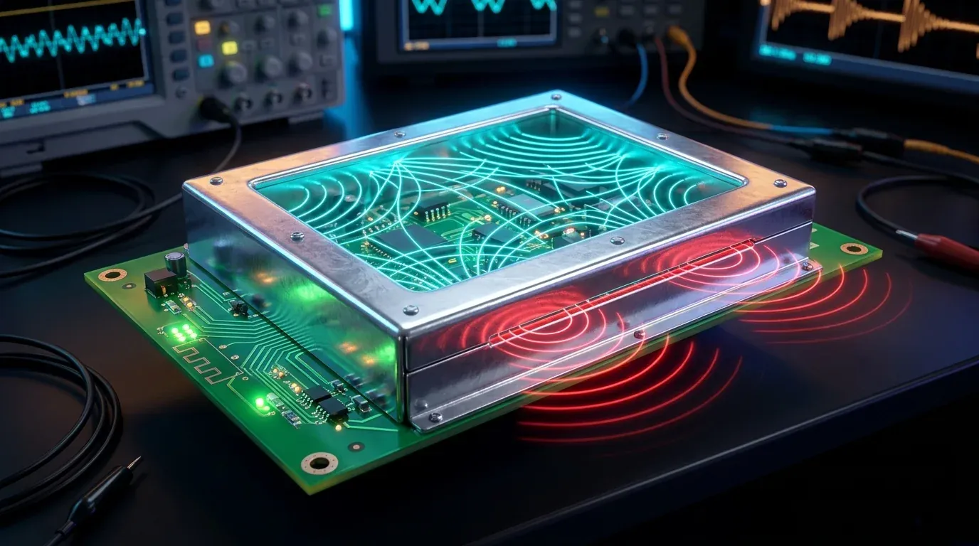
Therefore, mechanical engineers must place screws densely or use conductive gaskets at joints to ensure that the spacing between any two adjacent fastening points is less than of the wavelength corresponding to the highest frequency of concern.
For ventilation, simple perforated steel plates can only handle low-frequency disturbances below 50MHz. For high-frequency requirements, honeycomb vents operating as waveguide-below-cutoff should be introduced. A waveguide acts essentially as a high-pass filter. As long as the noise frequency is far below the cutoff frequency of the waveguide, the electromagnetic wave will decay exponentially within the waveguide tubes, achieving perfect isolation that allows airflow but blocks electromagnetics.
Level 4: Filter Design (Mitigating Conducted Emissions)
While shielding blocks spatial radiation, filters are the “chokepoint” to kill conducted disturbances. EMI filters are typically passive low-pass networks, but they operate under an extremely counter-intuitive physical principle.
Impedance Mismatch Maximizes Filter Insertion Loss
In communication RF circuits, we strive for impedance matching to maximize power transfer; in EMC filter design, we strive for extreme “impedance mismatch.”
The insertion loss of a filter depends heavily on the relative relationship between source impedance and load impedance. If the noise source impedance is low (e.g., a power supply), the filter input must present a high serial impedance (inductance); if the noise source is high impedance, the filter input must present a low parallel impedance (capacitance).
Common Pitfalls in Filter Installation
Even if you choose a filter with excellent specifications, its insertion loss can drop to zero instantly if installed incorrectly:
- Strictly prohibit input and output lines from running in parallel or crossing: High-frequency parasitic capacitive coupling (capacitive coupling ) or mutual inductive coupling (inductive coupling ) will allow high-frequency disturbances to directly bypass the filter.
- Metal-to-metal low-impedance grounding nearby: The Y-capacitors in the filter must divert common mode noise back to the reference ground. If the filter housing does not make direct, large-area metal-to-metal contact with the chassis and instead relies on a thin green-and-yellow wire for grounding, the high-frequency inductive impedance of that wire will completely choke the discharge path of common-mode interference.
Level 5: Transient Protection Design (Discharging Surge and ESD)
In real-world operations, equipment must withstand surge transients (Surge), electrical fast transients (EFT), and electrostatic discharges (ESD) of several kilovolts. These pulses are characterized by extremely high voltages and astronomical rates of current change ().
Residual Voltage Rise Under Transient High Currents
Faced with ESD, engineers typically place TVS (Transient Voltage Suppressor) diodes at the interfaces. Yet, during ESD testing in the lab, internal ICs still get damaged. Why?
The answer brings us back once again to the formula . Electrostatic discharge produces peak currents of tens of Amperes in a few nanoseconds. If your TVS diode has extremely long leads, or its ground via connects to the ground plane through a long trace, this tiny parasitic lead inductance will instantaneously induce a voltage drop of tens or even hundreds of Volts. The actual voltage clamped across the IC = TVS clamping voltage + lead inductance voltage drop. This is more than enough to destroy any precision digital IC.
Multi-Stage Coordination and Interface Physical Sequencing of Protection Devices
Different protection devices possess distinct physical genes and must be used in combination:
- Gas Discharge Tubes (GDT): Extremely high insulation resistance, tiny junction capacitance, and massive surge-handling capacity (tens of kA), but slow response times (hundreds of nanoseconds). Ideal for primary (coarse) protection.
- Metal Oxide Varistors (MOV): Large energy absorption capacity but prone to aging, with relatively large parasitic capacitance. Ideal for mid-level protection.
- TVS Diodes: Extremely fast response times (picosecond level) and precise clamping, but lower current-handling capability. Ideal for fine protection close to the IC.
In actual interface routing, a strict physical interception layout sequence must be followed:
External Interface Coarse Protection (GDT) Impedance Device (Common Mode Choke / Decoupling Resistor) Fine Protection (TVS) Filter Capacitor Sensitive PHY Chip.
Never place the TVS diode on the inner side of the common mode choke; otherwise, the massive transient current will directly puncture the winding insulation of the common mode choke.
Conclusion
Electromagnetic compatibility is never a “black magic” in the laboratory; it is rigorous, cold physics. From source control at Level 1 to transient protection at Level 5, every system crash and every out-of-spec frequency peak we encounter is a result of parasitic parameters, high-frequency impedance, and transmission line effects silently taking over the game.
In the era of high-speed, high-frequency modern electronic design, engineers can no longer afford to be mere trace routers (or netlist connectors) blindly following schematics and staring at idealized network nodes. Instead, we must elevate our thinking and evolve into “electromagnetic field architects” who control three-dimensional physical space. We need to learn to visualize the ground bounce brought by every switching transient, scrutinize the actual return path of every high-frequency signal, and remain vigilant against the common-mode antenna effects lurking within every external wiring harness.
Shifting EMC design upstream—from late-stage “rescue testing” to the very beginning of hardware R&D, and using physical laws to guide schematic component selection, PCB topology planning, and chassis structure design—is the ultimate way to avoid endless cycles of redesign in the lab. When you start to respect and align with these high-frequency physical laws, the seemingly wild electromagnetic fields will naturally reward your products with rock-solid stability.
Doing EMC or RF Testing?
Use our free online engineering calculators to instantly convert dBuV, dBm, VSWR, Antenna Factors, and more.